
- pcb design
- pcb legend
- board labelling
- electronics
- assembly
- dfm
PCB Legend Layer: What to Print on the Board
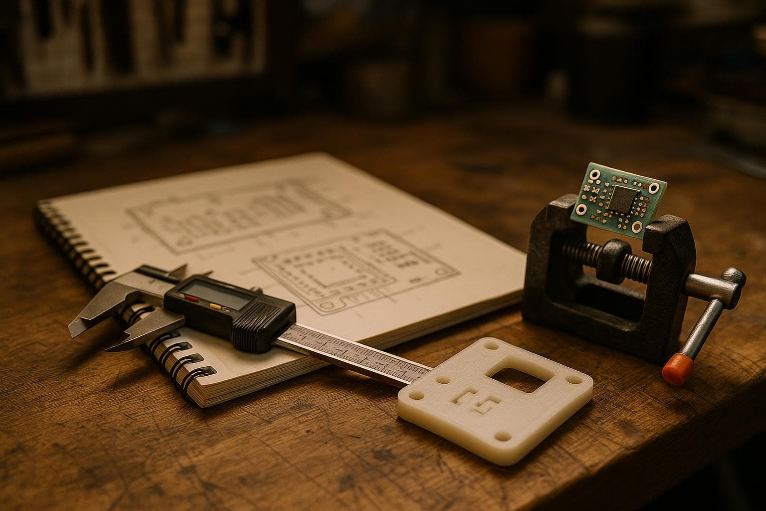
A bare board can pass every electrical test and still waste hours at assembly or service because nobody can tell pin 1 from pin 8. The honest answer is to print only the information that prevents a wrong connection, a wrong orientation, or a lost revision, then check every mark against the finished copper and assembly clearances before fabrication.
PCB legend space and mechanical clearance
A crowded board tempts us to put reference designators wherever there is an empty-looking patch. That patch may be reserved for a connector body, a clip, a probe, a rework tool, or the fingers needed to place a part. The result is a board that is electrically correct but awkward to populate and difficult to diagnose.
The first check is mechanical, not cosmetic. Import the actual footprints and enclosure constraints into the PCB layout, then inspect the board in the assembled state. Mark these areas as keepouts for board labelling:
- component bodies and their courtyard boundaries
- connector housings, latches, and cable exit paths
- mounting hardware, standoffs, and washer contact areas
- heat sinks, shields, batteries, and parts that may be replaced
- probe access areas around test points
- the solderable area of every pad
Printed legend over a pad is removed during manufacture. The board house clips or removes that legend from the solderable area, so a label placed over a pad may arrive broken, shortened, or absent. It must sit clear of the pad and its required clearance, not merely clear of the copper outline shown in a casual view.
Do not rely on final clipping to make a crowded layout acceptable. Turn on the manufacturer or design-rule check for legend-to-pad clearance, and review the generated fabrication artwork. The artwork is the check that catches a label disappearing before material and machine time are committed.
Orientation and polarity marks
A reference such as U3 tells us which part belongs in a location. It does not always tell us which way the part faces. That distinction matters for ICs, diodes, LEDs, polarized capacitors, connectors, and modules with asymmetric pinouts.
A useful pin-one mark is a filled dot, a short bar, or a clearly defined corner mark placed outside the component body and away from pads. Pick one convention and use it throughout the board. A notch or chamfer in the silkscreen can work for an IC, but only if it cannot be confused with a board edge, mounting hole, or nearby trace.
For polarized parts, print the electrical meaning as well as the physical orientation. A plus sign beside a polarized capacitor is more useful than a generic outline. A diode needs a cathode bar that matches the part marking. An LED needs both polarity and, where relevant, a note that identifies the cathode or anode convention used by the footprint.
Colour is not a reliable polarity legend. Red and black wires can be swapped, LEDs can be fitted in either orientation, and a dark board under poor light can make a subtle marking hard to see. A plus sign, minus sign, cathode bar, or explicit GND survives those conditions better.
Do not place a polarity symbol where it can be read as a pin-one mark. The symbol should sit beside the relevant pad or outline, with enough separation that its meaning is unambiguous after legend clipping. For a two-pin connector, label both pins if reversing the plug could damage the circuit. For a battery input, print the accepted voltage range only if it is a firm design requirement and will remain correct for that revision.
The check is to hide the schematic and inspect the board as an assembler would see it. Cover the courtyard and body labels if necessary, then ask whether each part can be oriented correctly from the board alone. If the answer depends on remembering a footprint convention, the marking is insufficient. Also perform a polarity walk from each power entry through protection, regulation, and load connections, comparing the route with every plus, minus, ground, and diode mark.
Connector and test-point labels
J4 is a reference designator, not a wiring instruction. A connector label that says only SENSOR or POWER leaves the next person to find the schematic, trace the board, or guess from wire colours. That is how signal and supply pins get swapped.
Print the signal name beside each connector pin when space permits. For a small connector, a compact order such as 1 GND 2 VCC 3 SDA 4 SCL is usually more useful than a large connector name. Include voltage where it distinguishes otherwise similar rails, such as 5V, 3V3, or VBAT. For a cable that may be inserted into a matching header, mark pin 1 at the board edge and show the mating orientation.
A connector pinout should describe the board side, not the cable side, unless the legend says so. This distinction matters with housings viewed from the wire-entry face. Verify pin numbering from the same viewing direction used in the legend, then compare every printed signal with the schematic and net names in the layout.
Use the cheapest clear marking that solves the problem. A large connector name plus a separate assembly sheet is good enough for a controlled build where the sheet stays with the unit. For serviceable or field-installed hardware, board-side pin names are worth the area because the sheet will eventually be missing.
A test pad without a label is just exposed copper. A label such as TP7 is better, but it still forces the technician to find TP7 in another document. Put the signal name beside the test point, and add ground or reference information where the measurement requires it. For analogue signals, include the expected function rather than an assumed voltage unless the voltage is fixed by the design. TEMP_SENSE remains correct across operating conditions; 1.20V REF is only correct if that reference is actually fixed. For a differential pair, mark A+ and A- or the project's chosen names. For serial interfaces, mark TX, RX, and GND from the board's perspective.
Keep the label outside the probe landing area. Probe tips need approach space, and a solder mask opening or test fixture may occupy more room than the visible pad. The check is a probe-access review using the real probe, pogo fixture, or test jig. If the probe touches a neighbouring pad before the intended one, move the marking and the point together.
Revision and date information
A board marked only Rev B is not a durable record. Revision letters repeat across projects, get separated from their repository, and lose meaning when a schematic is moved or renamed. A version and date printed on the board is what identifies a revision years later without a schematic.
Use a compact format that can be read in a photograph, such as CTRL Rev 2.1 2026-08. The project identifier prevents two boards in the same enclosure from being confused. The revision identifies the design state. The date gives a time anchor when filenames, repositories, or build records are no longer available.
Do not hide this information under a module or battery. Put it in a service-visible area, and repeat it on the underside if the board can be installed with that side inaccessible. Keep the date tied to the released fabrication data, not the date the board was ordered. If the layout changes without an electrical change, decide whether your document-control rules require a new version and apply that rule consistently.
The check is to export the final artwork and read the mark at the smallest expected service photograph or inspection distance. If the date becomes a blur, shorten the project identifier or move the text rather than shrinking it until it is technically present but practically useless.
Choosing a permanent marking method
| Marking method | Temperature exposure | Placement tolerance | Main failure mode | Cost per part |
|---|---|---|---|---|
| Fabricated PCB legend | Defined by the board house's legend ink process | Artwork and legend-clearance rules control it | Clipped from pads or hidden by a component | Usually part of board fabrication |
| Copper text under solder mask | Follows the board's copper and mask stackup | Limited by trace, mask, and clearance rules | Low contrast or covered by solder mask variation | Usually low incremental fabrication cost |
| Hand-applied label | Depends on label stock and adhesive | Depends on manual placement | Lifts, obscures access, or differs between units | Adds labour per board |
| Assembly document only | No board temperature limit | No physical placement issue | Document is separated from the board | Low part cost, higher service dependence |
For most boards, we pick the fabricated PCB legend for permanent orientation, connector, polarity, revision, and test-point marks. Copper text is a fallback for locations where legend space is tight, not a replacement for readable service information. Hand-applied labels make sense for a late change or a temporary prototype, but they are a poor permanent answer near heat, solvents, connectors, or moving cables. The cheap option of putting a clear pinout in the assembly drawing is good enough when the board will never be serviced separately; adding tiny unreadable text to every remaining gap fixes a problem that does not exist.
Pre-fabrication board-labelling check
Run this review on the final assembled view and the final fabrication artwork, not only on the schematic:
- Can pin 1, polarity, and connector orientation be identified without opening another file?
- Are every legend character and symbol clear of solderable pads and required clearance?
- Can a technician read the project, version, and date after the board is installed?
- Do connector labels describe board-side pin numbering and signal names?
- Are test-point labels outside probe and fixture access areas?
- Are labels hidden by components, shields, cables, standoffs, or enclosure walls?
- Has mirrored text been caught by checking the bottom copper and legend views?
- Does the exported Gerber or fabrication preview show the marks in the intended layer?
- Does the text still make sense if the schematic is unavailable?
Print a one-to-one artwork view if the board is dense. A screen zoom can make a marginal label look usable. A physical print exposes crowded symbols, reversed orientation, and text that is too close to a pad before the board is committed.
Should reference designators be printed beside every component?
For serviceable boards, print them for parts that may be replaced, tested, adjusted, or discussed in documentation. Dense passive arrays may need only grouped or abbreviated references if the assembly drawing provides the mapping. Never sacrifice pin-one, polarity, connector, revision, or test-point information to preserve every small designator.
How much clearance should PCB legend text have from a pad?
Use the board house's current legend-to-pad rule and design-rule file, because the accepted value varies by fabrication process and software rule set. Keep extra space where readability matters. Then inspect the generated legend artwork for clipping instead of assuming the rule check has preserved the whole character.
Is a date necessary if the board has a QR code?
Yes, if the code depends on a reader, database, or network that may not be available during service. A human-readable version and date remain useful when the code is damaged or the linked record has moved. The code can carry extra data, but it should not replace the basic identity printed on the board.
We build made-to-order custom electronics and design work through /quote.
Related services
All services →
Have a project in mind?
Tell us what you want built — we reply within 24–48 hours.